VLSI SoC / Physical Design using Open-Source EDA tools by The VSD corp. done on a cloud-based platform known as VSD-IAT, a user-friendly platform to learn and implement the essential skills in physical design using open-source EDA tools.
-
- Study various components of RISC-V microprocessor based SoC and review RISC-V picoSoC
-
- Running Pin Placement of picoRV32, understanding Floor Plan and Library Cells using the EDA tools
-
- Design and Characterization of cells using Magic Layout tool and ngspice
-
- Timing Analysis, Clock Tree Synthesis and Signal Integrity
-
- Final steps for RTL2GDS
I started working on the IC design component terminologies. An overview of the QFN-48 Package, layout of the chip, pads, core, die and IPs. RISC-V Instruction Set Architecture (ISA) was reviewed and the RISC-V flow was studied. The flow starts with the C/C++/Java code being converted to an Instruction Set Architecture (ISA) by the compiler and the assembler converts this ISA into binary. The RTL implementation is done using Hardware Description Language (HDL) to create a netlist which is then laid out on the chip.
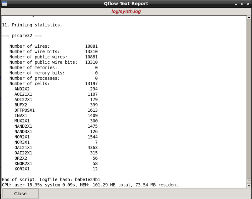
PicoRV32 CPU core was Analyzed. It is a is a CPU core that implements the RISC-V RV32IMC Instruction Set. It's Pin diagram and salient features were discussed before moving to the PicoSoC whose brief layout and features were then discussed. Raven SoC which is a slight modification to PicoSoC was discussed before moving out for the synthesis.
- Yosys : RTL Netlist to Logic Synthesis
- Graywolf : Floor Planning, Placement, Clock Tree Synthesis
- Qrouter : Routing
- OpenTimer : Static Timing Analysis
- Magic : Layout
- NGSpice : Pre-layout and Post-layout spice simulations
- eSim : Circuit Design and Simulations
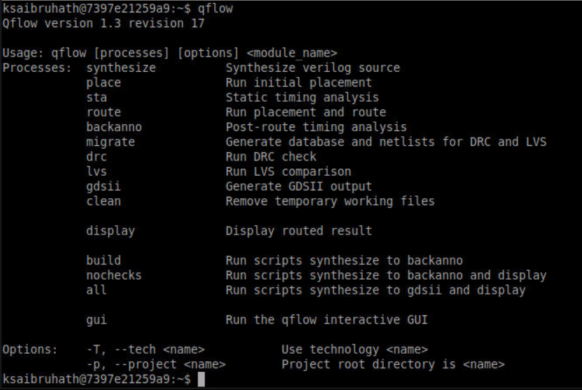
- Qflow : Tool Chain for complete RTS2GDS flow
The required tools were installed and working was checked with a sample design file.
Getting familiar with EDA Tools
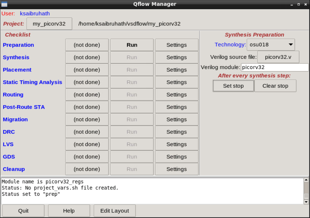
2. Running Pin Placement of picoRV32, understanding Floor Plan and Library Cells using the EDA tools
The dimensional analysis of the core and die of the chip were studied. Important parameters such as Utilization factor, Aspect Ratio which are important in understanding the design were studied. Various concepts crucial for Floor planning and placement like Pre-placed cells and & their advantage of enhancing reusability, Decoupling Capacitors and how they help the design were extensively discussed. A fully charged Decoupling Capacitor placed parallel to circuits to ensure proper supply of voltage and current by decoupling them from main supply voltage. This ensures proper local communication. The use of Power Planning, the concept of having a mesh of multiple Source and ground power lines, is made to ensure good global communication and avoid issues like Voltage droop and ground bounce. Placement strategies like, step of placing logical cell placement blockage to avoid Placement and Routing tool to place any other cells, usage of Buffers to recreate the signal were studied.
Library Characterization
The Inputs required by the characterization software are Process Design Kits (PDKs) which contain DRC, LVS Rules, Spice Models, Library and User-Defined Specifications such as the Width between the power lines (the cell height), drive strength etc. The Design step involves 'Layout design' and 'Characterization Flow'. The GUNA software takes the inputs and gives GDS2, LEF and extracted Spice netlist as Outputs. The Characterization is classified into Timing, Noise and Power Characterization.
Characterization Flow Steps
- CMOS Spice model file with basic parameters
- Extract the Spice Netlist
- Analyze the Circuit behaviour
- Read the Sub-circuit
- Read the Power Supply
- Apply proper Stimulus
- Provide necessary output capacitances (C_load)
- Provide necessary simulation commands
Timing Characterization
- Rise Delay : Time taken for waveform to rise from Slew Low Rise Threshold (20%) to Slew High Rise Threshold (80%) of VDD.
- Fall Delay : Time taken for waveform to fall from Slew High Fall Threshold (80%) to Slew Low Fall Threshold (20%) of VDD.
- Propagation Delay : Measured between 50% of Input transition to 50% of Output transition.
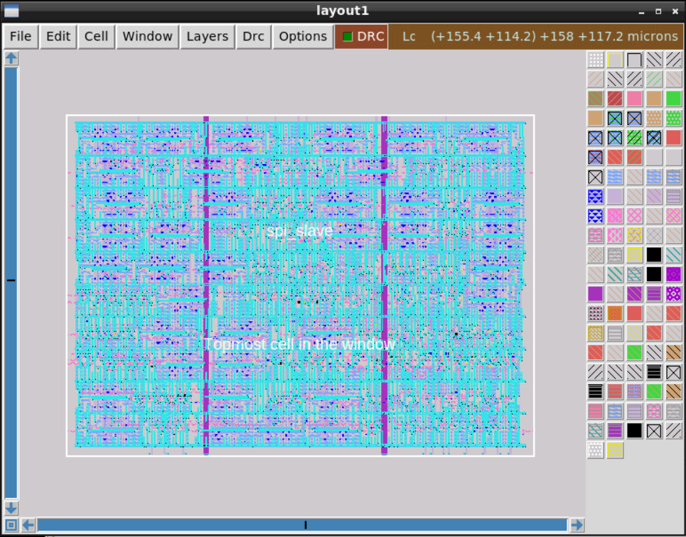
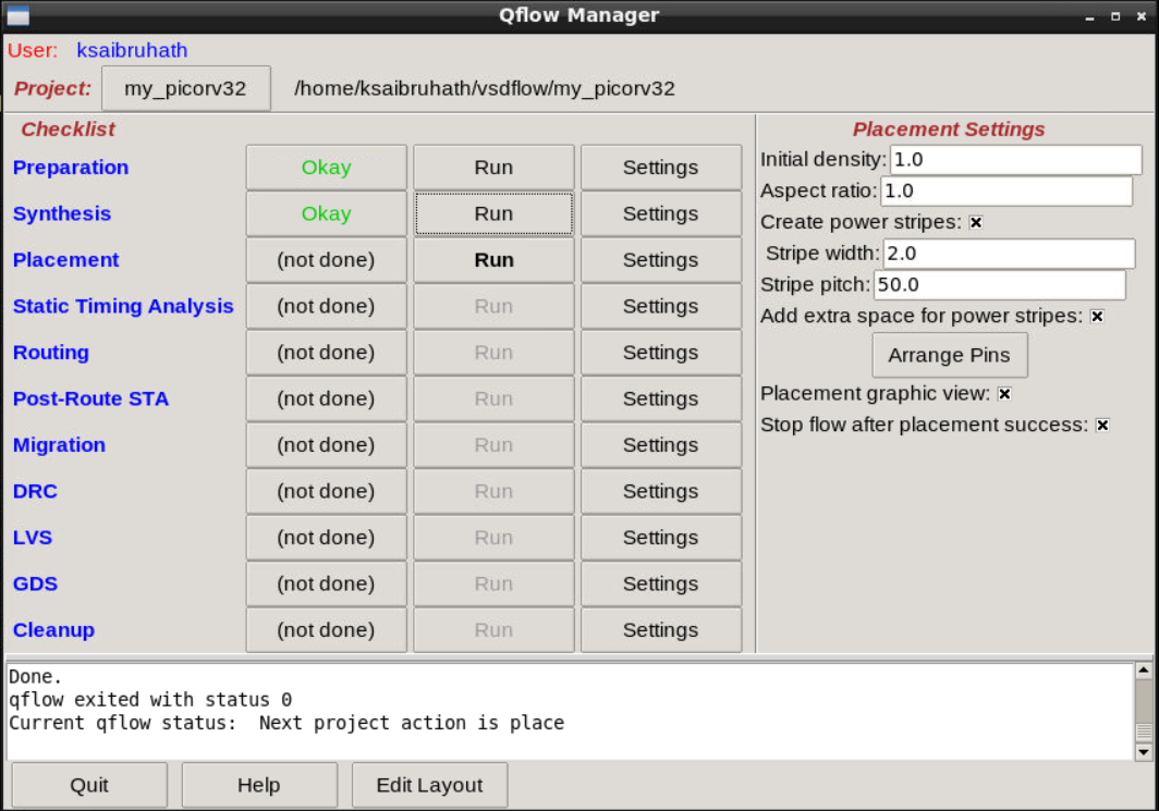
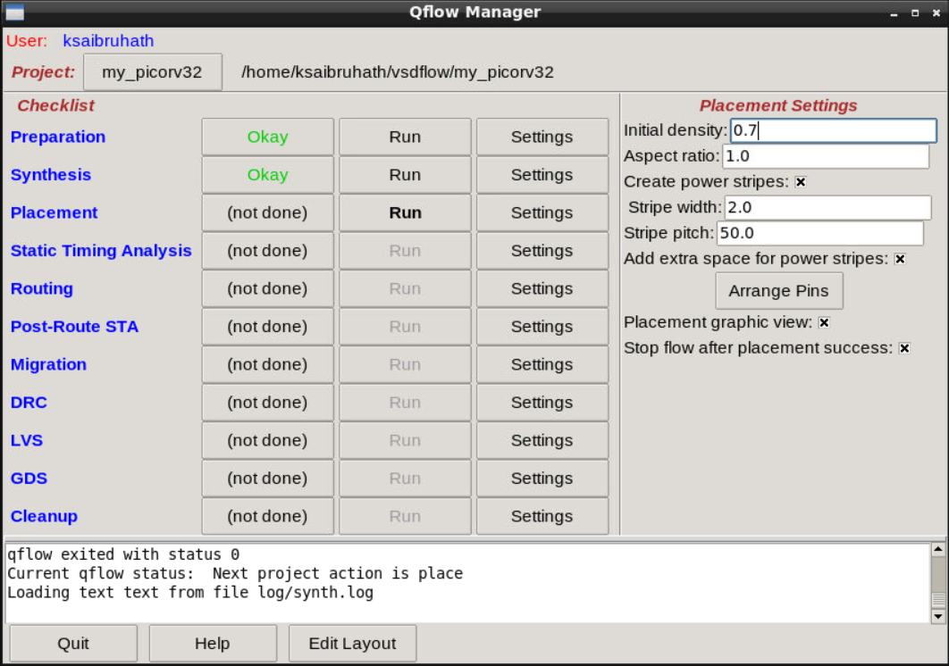
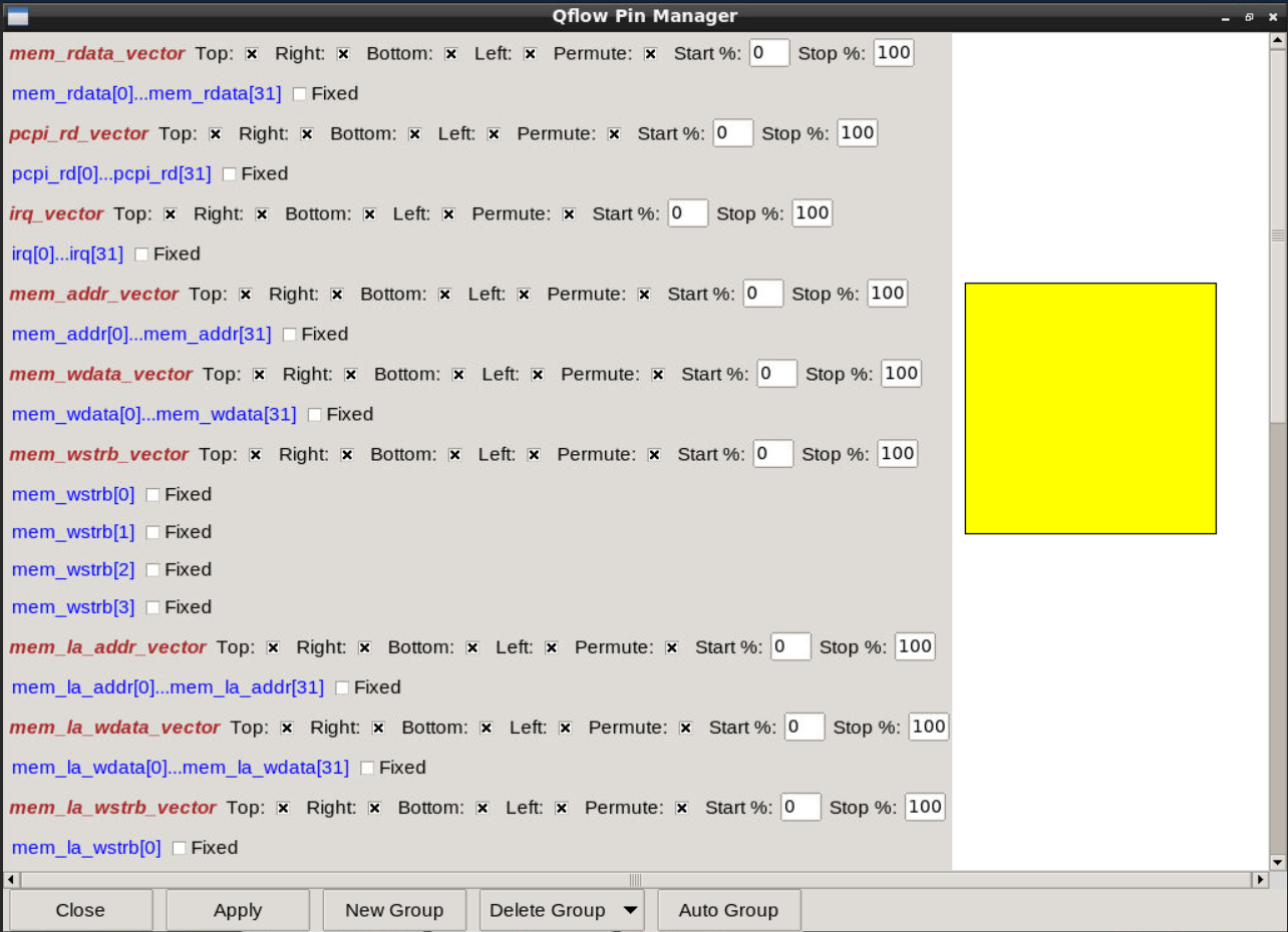
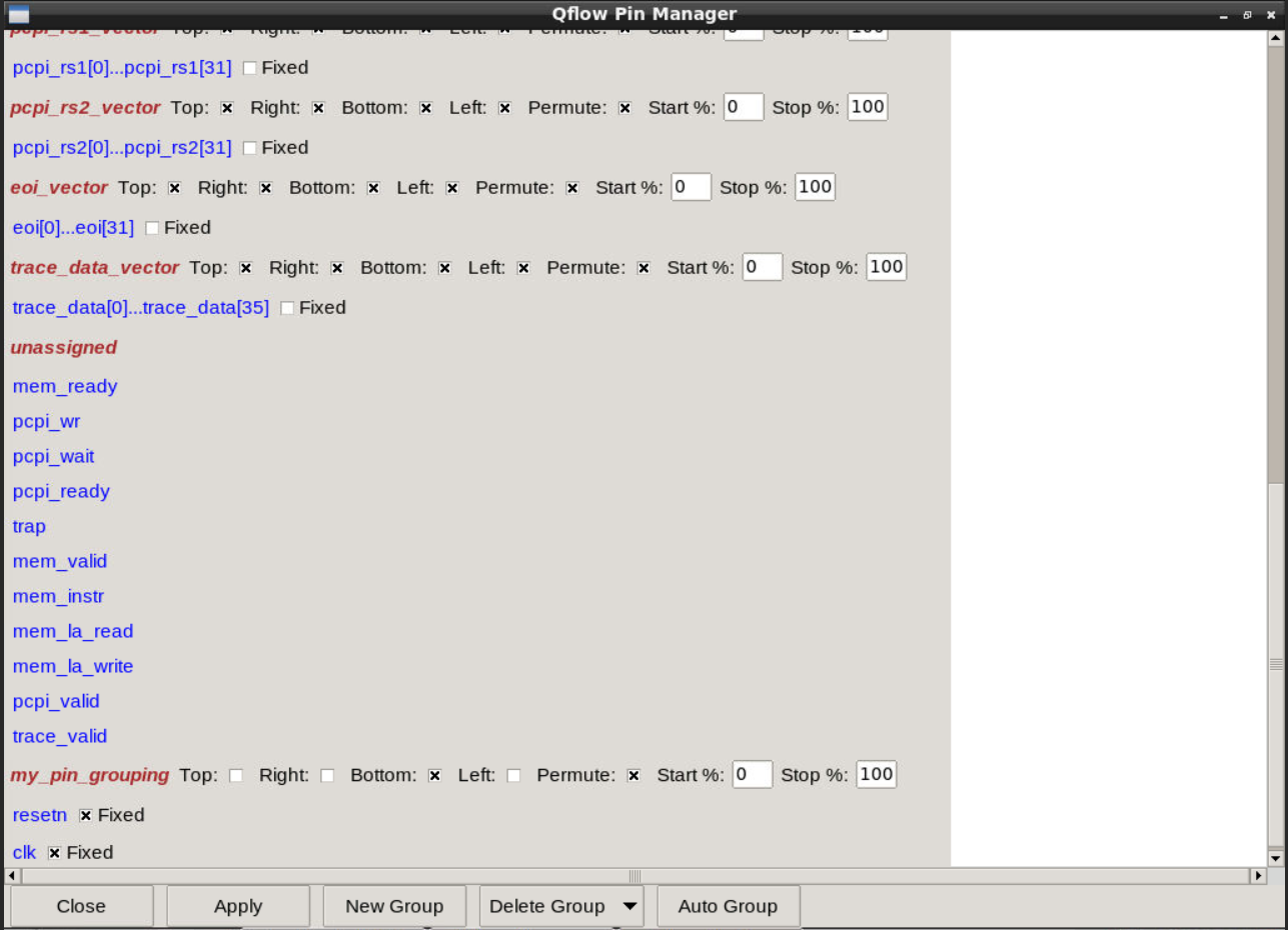
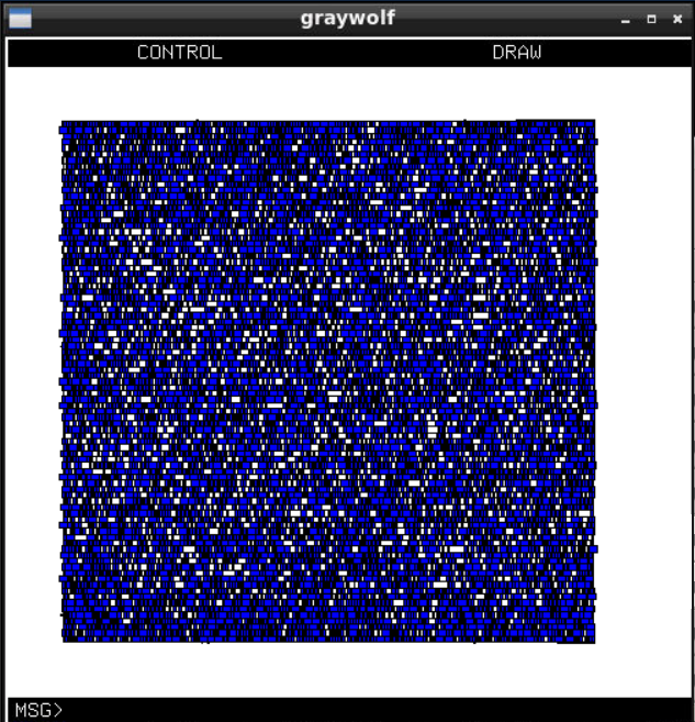
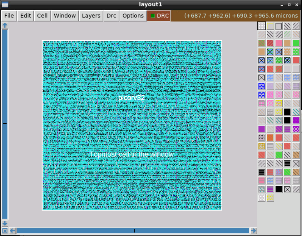
Continuing onto the Placement for picoRV32 after the Synthesis was done. Before proceeding for the placement, an understanding was made on Good and Bad Floorplan and placement methods. Keeping the design in point, analysis was done on where to put which ports, what are the ports that can be auto-grouped, which ports need to be added into a new group etc. After making the required changes to settings, placement was run and layout was analyzed.
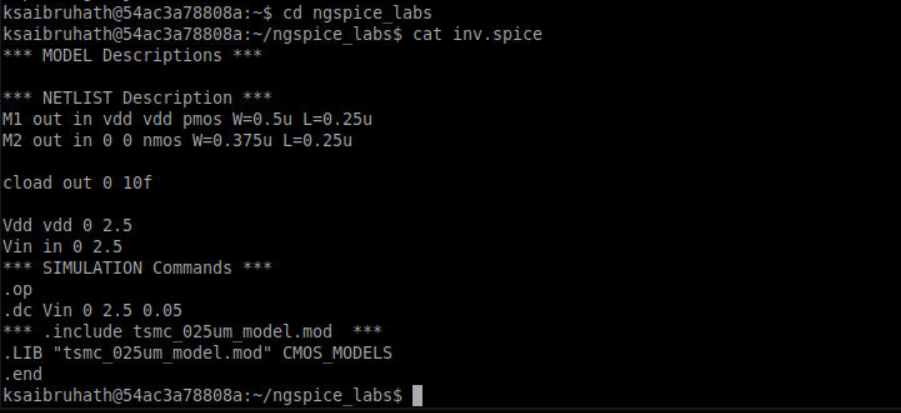
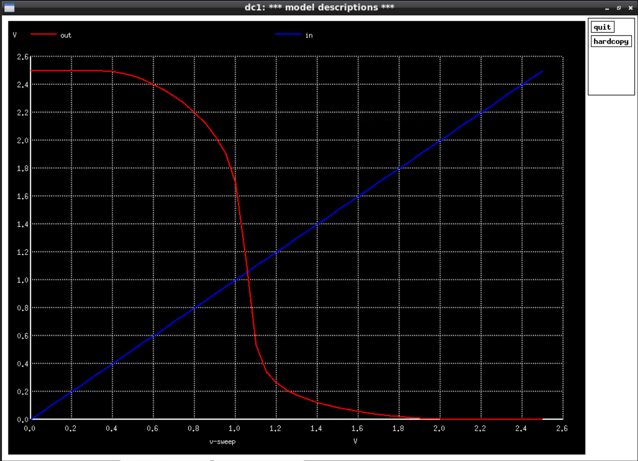
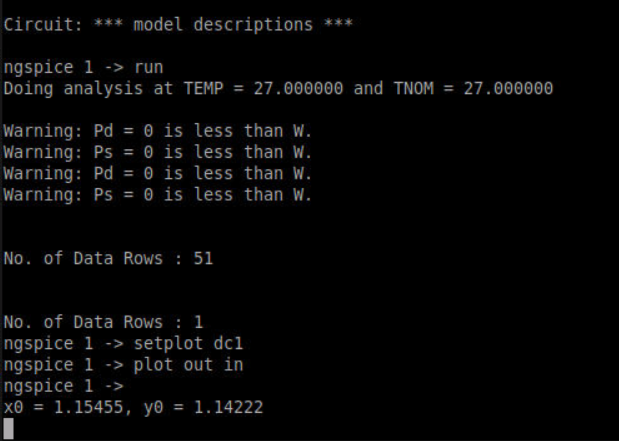
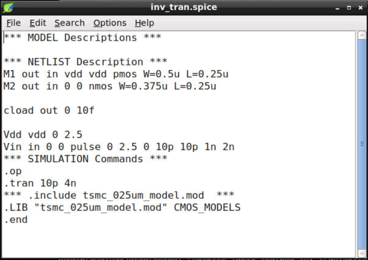
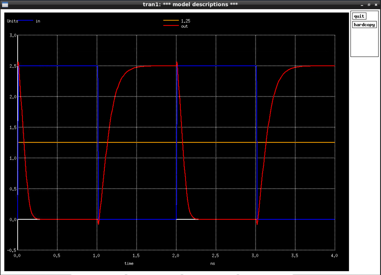
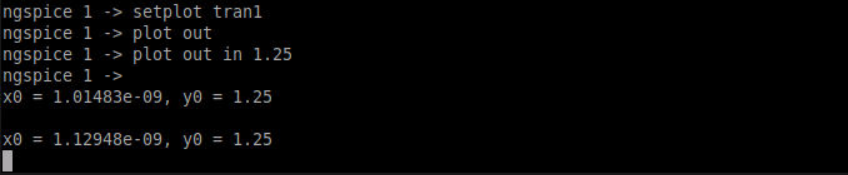
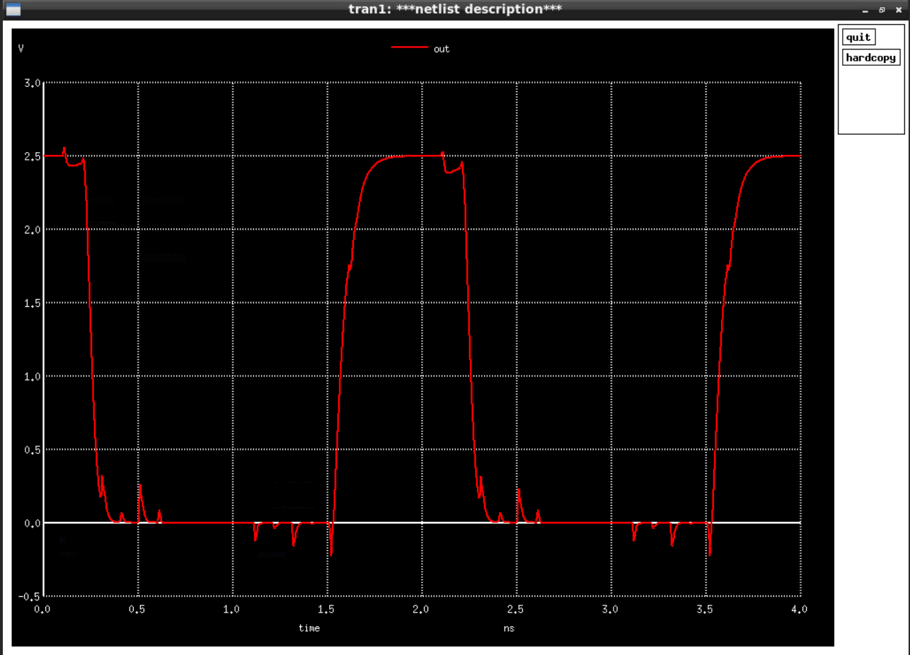
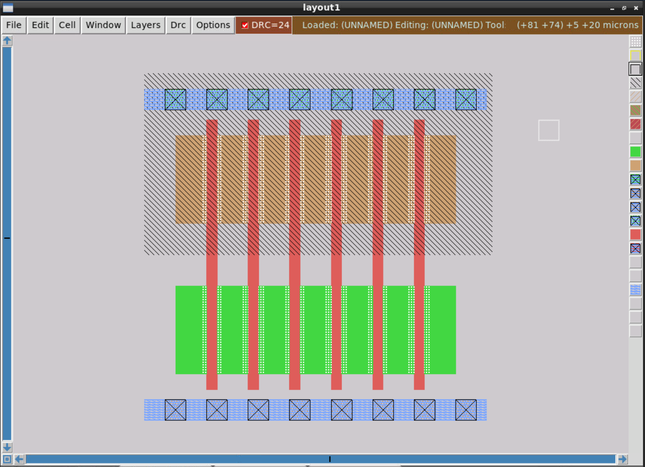
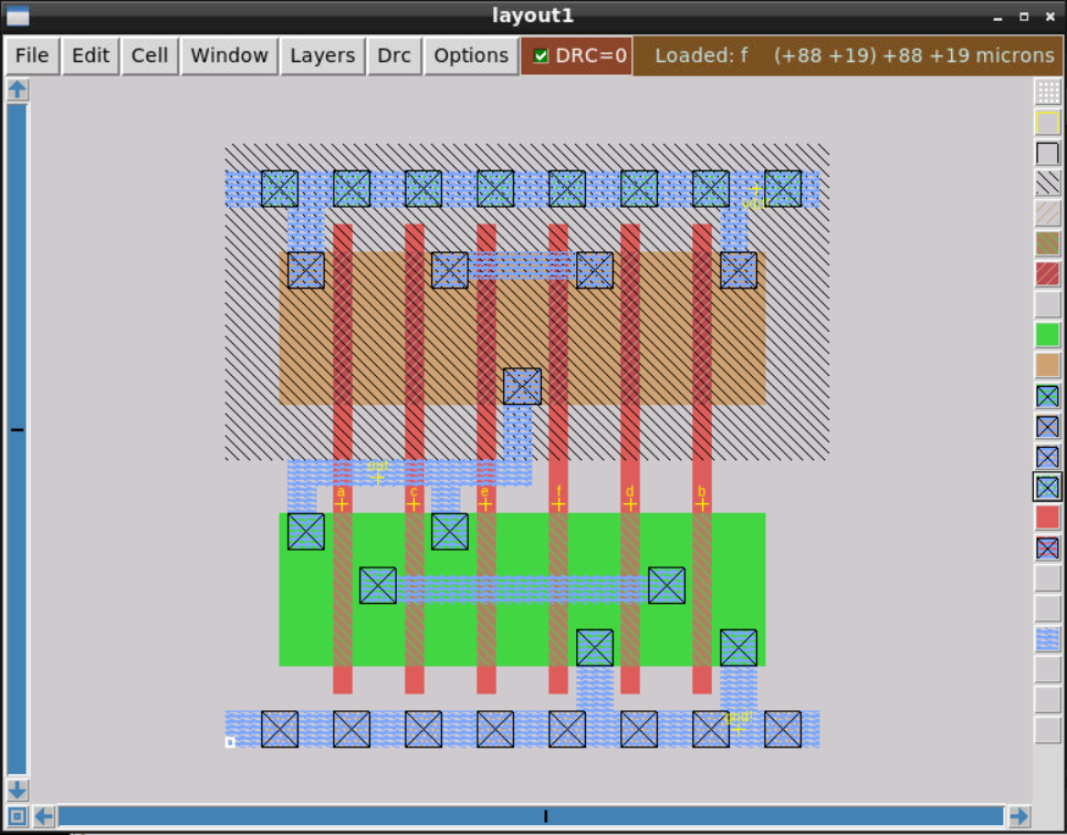
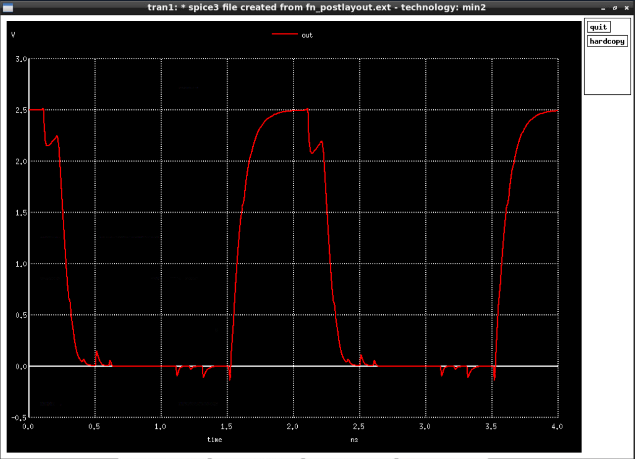
The usage of an important tool, ngspice was done. SPICE deck generation was learnt and practiced. Spice deck consists of the parameters of the CMOS design starting with the pMOS, nMOS source, drain ,gate voltages, dimensions (W, L) also including power supply along with simulation commands. W/L ratio of MOS impact on the performance was practically evidenced. The parameter Switching Threshold (Vm), deciding the robustness of the CMOS, was discussed. The concept of Stick diagram and Euler's path was studied and the impact of not considering the Euler's path was analyzed showing it's advantage of giving an optimal design. The layout with only Stick diagram was too clumsy and had too many metal contacts and connections. Considering each and every dimension, an extensive layout was designed.
MOS Netlist description in Spice deck
M1 out in Vdd Vdd pmos w=0.375u L=0.25u
M2 out in 0 0 nmos w=0.375u L=0.25u
cload out 0 10f

Vdd Vdd 0 2.5
Vin in 0 2.5

.op
.dc Vin 0 2.5 0.05

.LIB "tsmc_025um_model.mod" CMOS_MODELS
.end
Command for Transient Analysis
.tran 1n 20n
16-Mask CMOS Process
- Selecting a Substrate : A Substrate is selected to act as base layer over which other layers are formed.
- Creating Active regions for transistors : Silicon Dioxide (SiO2) and Silicon Nitride (si3N4) are deposited, pockets are created for P and N regions using Lithography.
- N-Well and P-Well formation : Ion implantation is done using Boron for P-well and Phosphorus for N-Well. Drive in diffusion is done by placing in high temperature furnace.
- Formation of Gate : Depending on the requirements of NA (Doping Concentration) and Cox (OXide Capacitance), lithography and ion implantation are done.
- Lightly Doped Drain (LDD) Formation : LDD regions are formed to avoid Hot electron effect and Short channel effect. Plasma anisotropic etching is used to leave small amount of oxide on side walls of Gate
- Source-Drain Formation : Very thin layer of oxide is formed over the top to prevent chanelling effect and, Source and Drain are formed using lithography and ion implantation.
- Forming Contacts and interconnects : Titanium is sputtered on the wafer surface and heated to form TiSi2 and TiN (2 types of metal contacts). Etching done by RCA Cleaning.
- Higher Level Metal formation : Planarizing the top surface, depositing upper metal layers.
The dependance of Delay of buffer on Input Slew and Output Load Capacitance was portrayed, and the concept of Delay tables which is based on those two parameters was extensively discussed giving the importance of 'levels of buffering', 'load driven by nodes' and types of buffer. The values not present in delay tables are extrapolated for precise results.
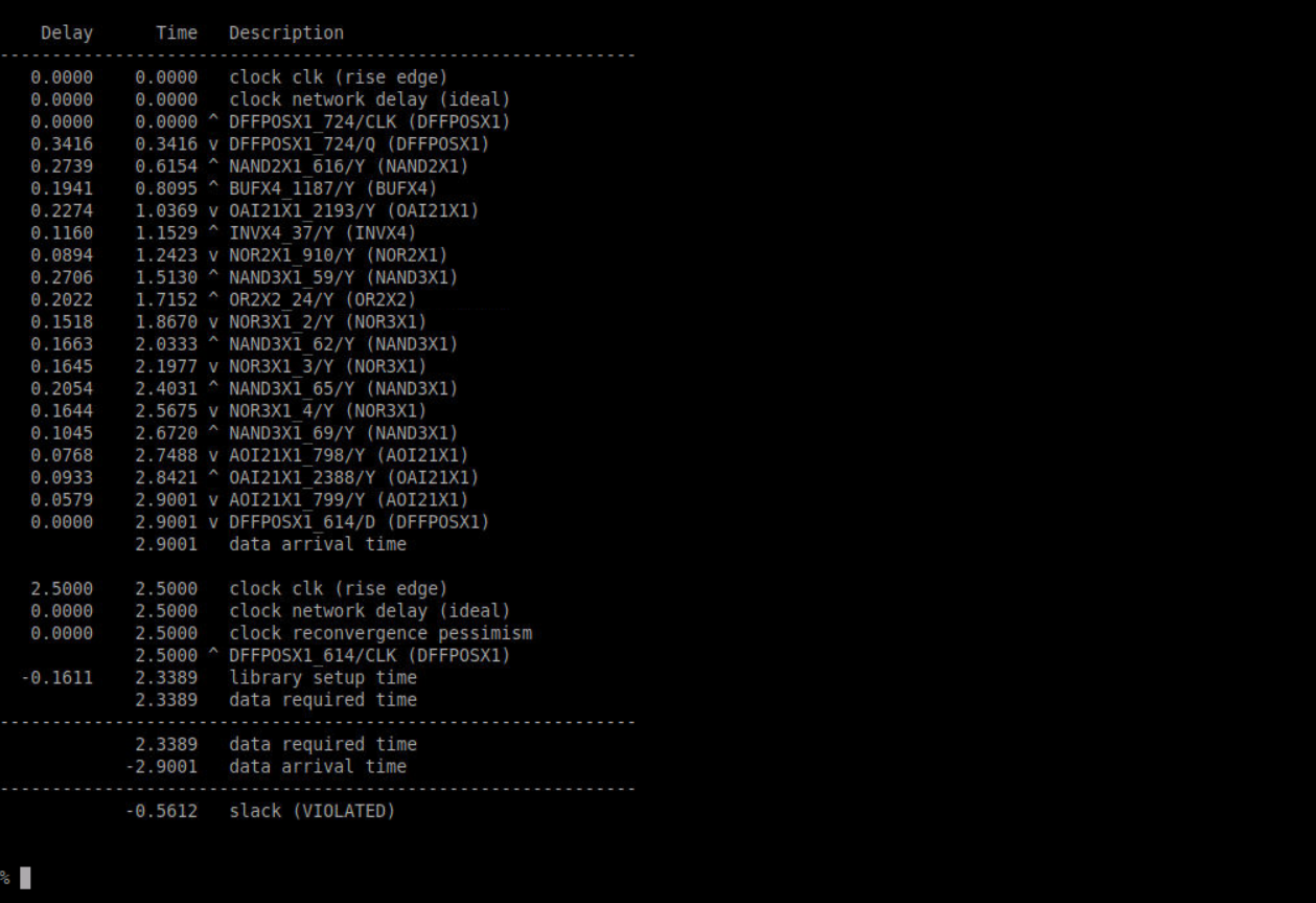
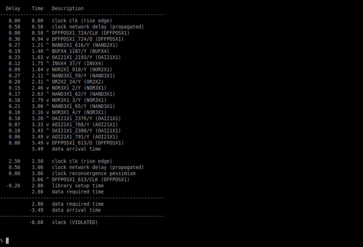
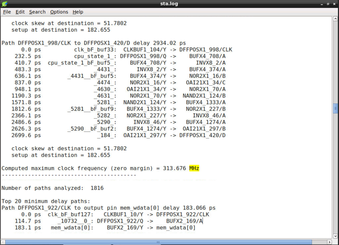
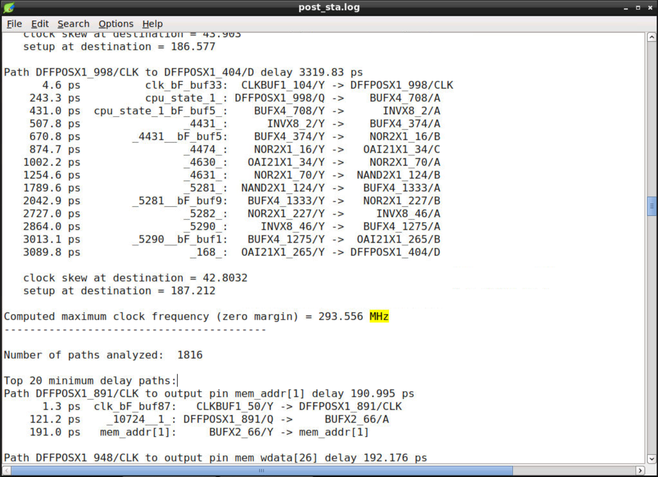
Setup & Hold Analysis with the concepts of library setup and Hold times, Setup and Hold Slack, Data Arrival and Data Required time were studied in detail keeping in mind the Jitter. A detail study was done on the concepts of Clock Tree Synthesis like H-Tree Algorithm and the importance of Clock Skew in it. The concepts of Victim and Aggressor in signal integrity, it's causes, effects, and remedies like shielding were analyzed.
- Setup time : The interval of time before the edge of the clock where the data should remain stable for data to get transferred properly.
- Hold Time : The interval after the edge of the clock where the data should remain stable for the data to get transferred properly.
- Setup Slack : The window by which the Setup requirements are being satisfied. ( Data Required time - Data Arrival time )
- Hold Slack : The window by which the hold requirements are being satisfied. ( Data Arrival time - Data Required time )
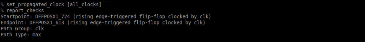
Commands to add Constraints in the SDC and Configuration files
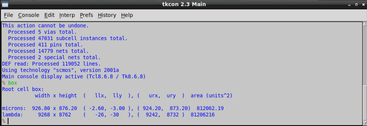
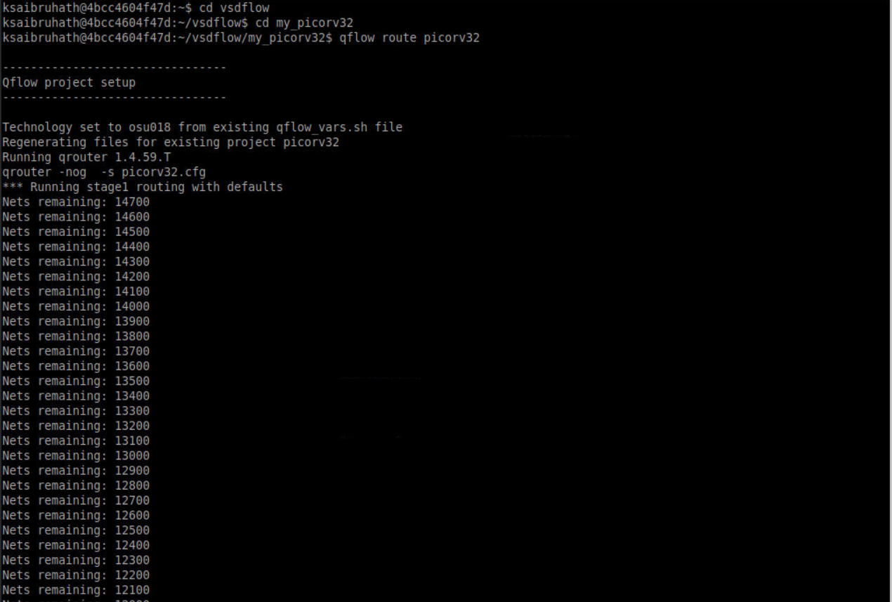
cd vsdflow/my_picorv32
leafpad picorv32.sdc

 // In the SDC File //
 create_clock -name clk -period 2.5 -waveform {0 1.25} [get_ports clk]

leafpad prelayout_sta.conf

 // In the Config File //
 read_liberty /usr/local/share/qflow/tech/osu018/osu018_stdcells.lib
 read_verilog synthesis/picorv32.rtlnopwr.v
 link_design picorv32
 read_sdc picorv32.sdc
 report_checks

sta prelayout_sta.conf
For Clock Propagation
set_propagated_clock [all_clocks]
report_checks
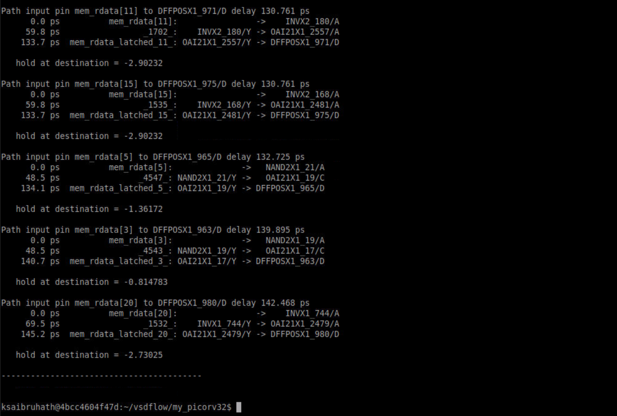
report_checks -path_delay min -digits 4
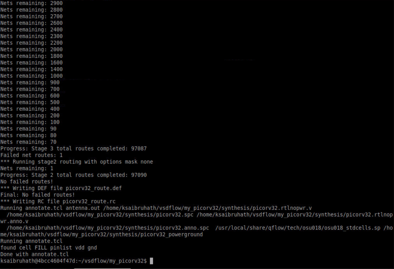
Starting with the concepts of routing, Maze Routing - Lee's Algorithm and it's advantages were studied, the algorithm generates a routing grid and labels it in such a way that, multiple possible routing paths are created and the best one is chosen. The DRC rules and considerations were discussed. The Parasitics Extraction in the SPEF (Standard Parasitics Exchange Format) IEEE 1481-1999 format, the SPEF Header and the representation of parasitics were studied in detail. In SPEF, the 'Port' details consists of name, it's type (Input/Output), Load, Co-ordinate, Driver, Waveform shape (rise/fall slew), and the 'Net' detail consist of Driver, Driver type, Receiver, Distributed Resistances and Capacitances.
SPEF Header format
*SPEF "IEEE 1481-1999"      // Format //
*DATE "xxx xxx xxx, xxx"    // Date of measurement of parameters //
*DESIGN "xxx"               // Design name //
*VENDOR "xxx"               // Vendor name //
*PROGRAM "xxx"              // Program name //
*VERSION "xxx"              // Version details //
*DELIMITER :                // Which Delimiter is used //
*T_UNIT 1ps                 // Time Scale //
SPEF format
*NAME_MAP
xxx         // Ports details //

*CONN
xxx         // Connection details //

*CAP
xxx         // Load Capacitances of net //

*RES
xxx         // Resistances of net //

*END
At the end, the complete RTL2GDS flow was successfully done using Open-Source EDA Tools.
RTL2GDS Flow
- Synthesis
- Floorplan and Power planning
- Placement
- Clock Tree Synthesis
- Signal Routing
- Sign-off
- Kunal Ghosh, Co-founder (VSD Corp. Pvt. Ltd)
- Nickson P Jose (VSD Corp. Pvt. Ltd)